 MSDS File
P-type Silicon Evaporation Materials Description
Silicon is a crucial metalloid with a melting point of 1,410°C and a density of 2.32 g/cc. At a temperature of 1,337°C, its vapor pressure is approximately 10^-4 Torr. This element is known for its brittle nature, making it prone to chipping. Silicon serves as a fundamental semiconductor in the electronics and computing sectors, where it is commonly doped with elements like arsenic, phosphorus, or boron, depending on the specific requirements of the application.High-purity P-type silicon evaporation materials are essential in various deposition processes, ensuring the production of high-quality thin films. TFM specializes in manufacturing silicon evaporation materials with purity levels reaching up to 99.999%. Their rigorous quality assurance protocols guarantee the reliability of these products.

P-type Silicon Evaporation Materials Specification
| Material Type | P-type Silicon |
| Symbol | Si |
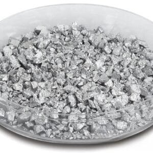
| Color/Appearance | Dark Gray with a Bluish Tinge, Semi-Metallic |
| Melting Point | 1,410 °C |
| Density | 2.32 g/cc |
| Thermal Conductivity | 150 W·m-1·K-1 (25°C) |
| Thermal Expansion | 2.6 x 10⁻⁶/K (25°C) |
| Bulk Resistivity | 0.005-0.020 OHM-CM |
| Synonyms | P-type Silicon Pellets, P-type Silicon Pieces, P-type Silicon Evaporation Pellet, P-type Si Pellets, P-type Si Pieces, P-type Si Evaporation Pellet |
P-type Silicon Evaporation Materials Application
P-type silicon evaporation materials are utilized in several advanced processes, including:
- Semiconductor Fabrication: Vital for the production of integrated circuits and other electronic devices.
- Chemical Vapor Deposition (CVD): Employed in creating thin films for various applications.
- Physical Vapor Deposition (PVD): Used for depositing materials in a vacuum environment, crucial for device manufacturing.
P-type Silicon Evaporation Materials Packaging
These materials are available in multiple forms, such as powders and granules, and can be customized to meet specific size and purity requirements. TFM’s commitment to handling these materials with care ensures that they maintain their integrity during storage and transport.
Get Contact
TFM offers a diverse range of P-type silicon evaporation materials, available in various forms, purities, sizes, and pricing options. Our focus is on producing high-purity e-beam evaporation materials that achieve the highest possible density and the smallest average grain sizes, ensuring optimal performance in your applications.


Reviews
There are no reviews yet.